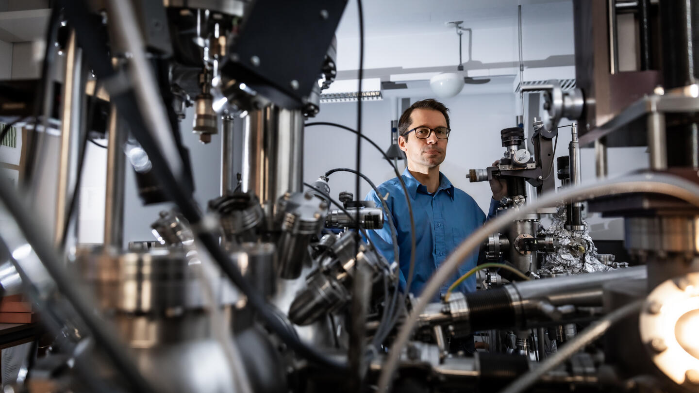
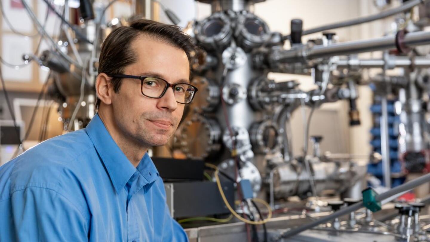
Pekka Laukkanen Develops Materials for Industries at Atomic Level
The materials scientists of the University of Turku solve industrial challenges and expand our understanding of the properties of materials. In his research, University Research Fellow Pekka Laukkanen concentrates especially on semiconductors. Researchers at the Materials Research Laboratory create new solutions for future industry.
The invention of transistor was one of the great technological leaps of the humankind. It enabled the smaller size and cheaper price of different technical gadgets. We all have in our pockets a phone whose microprocessor is a circuit chip only slightly bigger than the tip of a thumb and consists of billions of nano-scale transistors.
Silicon, the fourteenth element in the periodic table, is the basic material of all modern electronics. It has properties that work well with the semiconductor industry – it is cheap, durable, and non-toxic. Even up to 90 percent of all electronic devices include silicon.
– However, silicon does have some weaknesses. For example, it cannot be used to efficiently produce light, which means that it cannot be used in leds or lasers. By placing different types of semiconductor films on the surface of silicon, it is possible to modify its properties so that they are more desirable, tells University Research Fellow Pekka Laukkanen.
Laukkanen’s research has mostly centred around the surfaces of semiconductor crystals and their atomic-level properties. Although semiconductors might be a fairly unknown topic to many, everyone uses the technologies enabled by semiconductors countless times every day.
– Semiconductors are the basis of all modern electronics because their electrical conductivity can be regulated in a controlled way. They are also one of the most important materials in photonics. In addition to transistors, they enable the production of leds, lasers, different kinds of sensors, and solar cells, Laukkanen tells.
Laukkanen works in the Materials Research Laboratory lead by Professor Kalevi Kokko, where surface research is combined with the semiconductor technology. By combining the traditionally separate research fields, it is possible to create even better semiconductors. In many electronic appliances, the semiconductor surfaces in particular are the weak spots causing electrical malfunctions and shortening the life span of the applications.
– We aim to improve the understanding of these surface properties and find ways to modify the surfaces in a controlled way to decrease energy loss. This helps us to design more efficient solar cells, quicker transistors and, for example, computer processors that don’t heat up as much and are more energy-efficient.
From Research to Business
Laukkanen works at the Department of Physics and Astronomy in the Materials Research Laboratory. He directs an Academy of Finland project which ends next year and centres around the study of oxidation of semiconductor crystals and how the phenomenon affects the properties of surface layers. Uncontrolled oxidation has been an eternal problem in semiconductors.
– Oxidation is such a strong reaction that it often breaks the structure of the surface. Semiconductors are primarily crystalline materials while oxides are amorphous. If a crystalline semiconductor is turned amorphous due to oxidation, it can easily lead to malfunctions in electronics, Laukkanen tells.
In industry, these kind of malfunctions can be expensive. The researchers at the Materials Research Laboratory made a significant finding a couple of years ago when they managed to oxidise semiconductor surfaces in a controlled way utilising vacuum technology.
– When a semiconductor is oxidised in advance in controlled circumstances, the amount of defect levels in devices decreases and the performance improves, Laukkanen says.
The new oxide-coated semiconductor developed at the Materials Research Laboratory was named Kontrox. To commercialise it, Comptek Solutions Ltd. was founded in 2017. Two out of the three main founders of the company have a doctorate in physics from the University of Turku and have helped develop the technology.
– The support of the University in patenting the innovation and launching the business was crucial, says Laukkanen.
Afterwards, the company has raised a significant seed funding and exports the new technology to e.g. China. Laukkanen himself is not on the company’s payroll, but operates as an unofficial technological consultant.
– Four former postgraduates whose doctoral dissertations I supervised work in Comptek. We have good dialogue and co-operation with them. Often, the problem is that even significant research findings are not developed further for industry. Our laboratory was lucky because we had young researchers who are interested in entrepreneurship. I think that their enthusiasm, the high level of skills, and good work morale create a good basis for the success of the start-up.
Wide-ranging Materials Research
In addition to the Materials Research Laboratory, many other units and research groups at the University conduct high-quality materials research. At the Department of Physics and Astronomy, the laboratories of Wihuri and industrial physics concentrate on material physics while the Department of Chemistry has its own research groups for unorganic and organic materials chemistry.
– The materials research at the University is very extensive which offers exceptionally good collaboration opportunities, Laukkanen praises.
The groups also collaborate with different universities and research units. For example, together with the Aalto University, the Materials Research Laboratory develops new and more efficient solar cells which are expected to revolutionise the production of solar energy.
– Here in Turku, we are in a very good position in the sense that we can conduct high-quality materials research from the start of the production line to the finished product, or all the way from theory to practical tests. In this, the University’s investments on high-quality research environments have had a great impact, Laukkanen says.
Laukkanen tells that in addition to the research work, he also teaches. As the University of Turku is now expanding its technology education, Laukkanen will be also teaching the new technology students in the future.
– There is a genuine need for technology education because many industrial challenges are related to the properties of materials. Materials science and technology help us to build even stronger ships and more durable technologies at the businesses in the region.
Pekka Laukkanen
|